3D printing augmenting the traditional way of producing printed electronics
By Amritpal Singh Bedi, Sr. research associate, MarketsandMarkets research
Electronics Production / Materials Regulations & Standards Engineering Supply Chain 3D printing 3D printing printed electronics printed electronics3D printing, also known as additive manufacturing, rapid prototyping, or freeform fabrication, is a process in which three-dimensional complex-shaped solid objects are made by forming layers of materials such as polymers, metals, ceramics, paper and certain edibles (e.g., chocolate). The capability of this “additive manufacturing” has already surpassed the imagination of every industry. There is hardly any industry untouched by the knowledge of 3D printing technology. 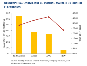
Technology overview
Three-dimensional (3D) printing is the process of building a 3D object from a digital model by joining thin layers of materials (which might be in solid, powder, or liquid forms), usually layer upon layer, in horizontal cross-section as opposed to the subtractive manufacturing methods. Based on the printing process, 3D printing can be classified into binder jetting, direct energy deposition, material extrusion, material jetting, powder bed fusion, sheet lamination, and vat photopolymerization. Material extrusion is the most commonly used 3D printing process in which a nozzle is used. In this process, the plastic material is heated and deposited in a layer-by-layer manner. The fused filament technology, most commonly known as fused deposition modeling (FDM), is used in the material extrusion process for 3D printing. Aerosol Jet Printing (AJP), Light Beam Sintering (LBS), Selective Laser Sintering (SLS) are some of the popular printing technologies used in printed electronics.
3D printing ushering in an era of printed electronics
The 3D printing technology allows engineers and designers to design and prototype novel devices, such as 3D-printed antennas, sensors, actuators, and coils and to stack integrated circuits in ways that weren’t previously possible. These quick-printed circuit boards may offer ways for niche markets to make inexpensive, even flexible circuit boards and to prototype quickly so that the user wouldn’t have to wait for economical boards to come from China or order expensive boards from the US. Therefore, if users want to build a prototype or produce a small batch of some complex electronic circuitry, they can easily get it done with the help of 3D printing technology.
This technology further provides complete control over shapes and other physical attributes of printed electronic components to cater to the requirement of a particular product, thereby optimizing the design for better functionality. By following this “additive manufacturing” approach, rather “subtractive manufacturing” one, users have full control over the design and manufacturing process at their fingertips. This significantly enhances the quality of a product by narrowing the gap between the decisions regarding the implementation of any essential last-minute change and actually getting it done. According to MarketsandMarkets research, the 3D printing market for printed electronics industry is expected to be valued nearly USD$1-billion by 2023 growing at a CAGR of over 30% between 2017 and 2023.
Business model and its impact on the bottom line
3D printed electronics are majorly used in printed circuit boards (PCBs) on a flexible substrate for the simple construction of conductive patterns. Although currently available printed electronic devices are not ‘fully 3D-printed’ electronic devices, PCB designers, by using the 3D-printing technique, can shorten their prototyping time for sure. The term is interchangeably used for several applications, the most common being the fabrication of passive components (resistors, inductors, capacitors) and circuits (filters, waveguides) by using available 3D printing techniques utilizing advanced nanoparticle conductive metal inks or polymers that are subsequently metalized. Another common usage of 3D printing across the printed electronics ecosystem is based on jetting the ink containing metal particles or a low-melting-temperature metal/metal alloy and creating conductive tracks, antennas, passive filters, and so on.
3D printing is still regarded as a planar technology, some active components, such as transistors, can be printed either by superposing organic semiconducting layers having different types of conductivity (p, n) or by using the field effect. This method has been successfully deployed for the creation of printed solar panels and displays, by printing organic compounds and by creating some sort of transistors and diodes, for example, OLEDs. But, 3D printing is still considered incipient for the creation of an array of other electronic components and for the successful transition toward making it a ‘production tool’ in the electronics industry rather than just a ‘prototyping tool.’
Many players associated with 3D printed electronics are currently focusing on 3D printed integrated circuits (ICs), not necessarily very complex as in the case of multi-layered circuits, that have performance close to that of similar Silicon-based ICs. Optomec (US), Nano Dimensions (Israel), Neotech AMT GmbH (Germany), Graphene 3D Lab, Inc. (US), Voltera (Canada), BotFactory, Inc. (US), and Cartesian Co. (US) are some of the providers of 3D printing technology (products and related solutions) to printed electronics OEMs and other associated market players. Currently, the market speculations are toward 3D printing micro-optical components and photonic integrated circuits (PICs), practical realization of which is currently restrained by certain challenges such as a quite limited range of materials.
The market of printing organic and flexible electronics using traditional printing methods (such as photolithography, flexography, screen printing, and others) is well-established, while the scope of 3D printed electronics has started shaping up with the successful deployment inside smart devices and IoT platforms, practical applications of which are multitudinous across consumer electronics, automotive, aerospace, defense, medical devices, drones, power generation, and several other end-user industries. Engineers and scientists are continuously increasing efforts toward R&D activities to further increase the scope of 3D printed electronics. For instance, Missouri University of Science and Technology demonstrated a creation of “stretchable” electronics, which can be embedded inside electronic gadgets, onboard systems of vehicles, fitness trackers, skin patches, smart clothes, and various other products. Such developments are further expected to unleash new design possibilities in the nearest future.
Underlying pros and cons and future perspectives
3D printing not only provides cost-efficient means to verify the proof of concept during the initial product development stages (compared to the standard silicon technology) but it also reduces the time to market printed electronics. Creation of 3D printed ICs, micro-optical components and photonic integrated circuits (PICs) are currently most demanding application area across this industry. Players in the 3D printing market are facing certain challenges, such as the creation of printed electronics at micro-nanoscale, with a resolution of just a few tens of nanometers, which need to be overcome. Research and developments are already testing the concept of Micro-Electro-Mechanical Systems (MEMS) technology-based devices.
The limited characteristic features of printing materials and need to drive down the overall cost of 3D printed electronic devices are some additional factors that hinder the 3D printing market growth. Other challenges are associated with the object size, spatial resolution, surface finish, palette of materials, functionality (especially conductivity of printing materials), less post-processing, material/structure properties, and fabrication speed. The lack of process standardization, miniaturization, and creation of more complex 3D shapes at micro-nanoscale, and creation of active components (transistors, either bipolar, unipolar, or field effect) are some of the other challenges.
Fully printed microprocessor technology
3D printing has not yet realized as a fully printed microprocessor technology. However, starting with the small-to medium-scale production of less demanding ICs (such as less complex controllers, sensors, and audio amplifiers), and then shifting toward realizing economies of scale will surely uncover the true potential of 3D printing technology. This would help in de-centralizing the current IC fabrication ecosystem, which is currently confined to big companies having strong financial capabilities. In contrast to the traditional fabrication methods requiring fabrication, assembling, and quality inspection of different individual parts and components of an electronic device from different places, 3D printing can realize the full system in just one run. Thus, the usage of a significant amount of workforce in traditional printing and fabrication approach (such as lithography) becomes disposable, thereby retrenching associated production costs.

Amritpal Singh Bedi, Sr. research associate, MarketsandMarkets research
Also, the lower impact on the environment resulting from minimal material wastage, elimination of the need for harmful chemicals used for “etching” during electronics manufacturing, and efficient energy consumption represents a direction of interest for 3D printing of ICs. Thus, 3D printing currently seems propitious for future mass customization and product development needs of the printed electronics industry.